Technological advancement has been successful in
miniaturizing components and structures in electronics to such a degree that
they are on the order of a billionth of a meter. Central to engineering
these nano-components is understanding the properties of
phonons.
Mapping phonons - a quantum of energy quasiparticle
associated with a compressional wave - in nanostructures is indispensable to
the development and understanding of thermal nanodevices, modulation of thermal
transport, and novel nanostructured thermoelectric materials. In crystals,
which hold an ordered atomic structure, these phonon waves of atomic
displacements tend to carry thermal energy equal to their freq
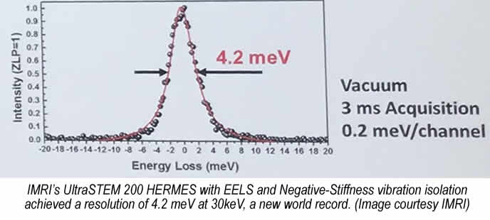
A New World Record in
Resolution
|
Through the
engineering of complex structures such as alloys, nanostructures and
superlattice interfaces, it is possible to alter their thermal conductivity by
controlling the propagation of phonons while maintaining electrical
conductivity. To achieve high phonon impedance it is optimal for nanostructures
to have an abrupt change in structure which lowers their
conductivity.
Studying Phonon Behavior
Utilizing an alloy of
germanium and silicon, a research team consisting of UCI's IMRI, the
Massachusetts Institute of Technology (MIT), and other institutions, was
capable of studying how phonons tend to behave in the disordered surrounding of
the quantum dot - the interface between the quantum dot and the encircling
silicon, and next to the dome-shaped surface of the quantum dot nanostructure
itself. Quantum dots are semiconductor particles a few nanometers in size with
optical and electronic properties that differ from those of larger particles
via quantum mechanical effects. They are a central topic in nanotechnology and
materials science.
|

|
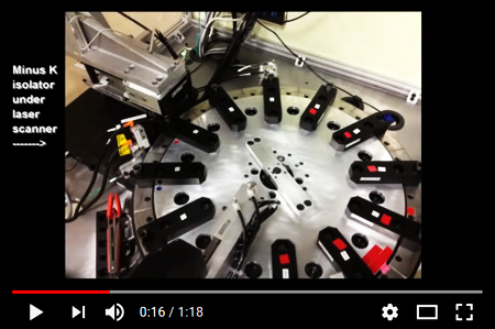
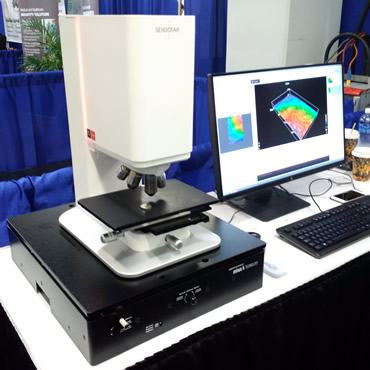
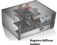
With the help of a
Nion UltraSTEM 200 scanning transmission electron microscope (STEM), the
research team has developed a novel technique to map phonons in crystal
lattices at atomic resolution. To examine how phonons are distributed by the
interfaces of Si/SiGe (silicon-germanium heterostructure) quantum dots, the
team probed the dynamic behavior of phonons next to a single quantum dot of
silicon-germanium utilizing vibrational electron energy loss spectroscopy
(EELS) in the STEM at IMRI. EELS is a technique that measures the bonding
environment of molecules with high spatial resolution.
"We developed a
novel technique to differentially map phonon momenta with atomic resolution,
which enables us to observe nonequilibrium phonons that only exist near the
interface," said Dr. Xiaoqing Pan, UCI professor of materials science and
engineering, and physics,"One of the really hard problems in solution-processed
organic devices is to develop methods to pattern the organic semiconductor on
the nanoscale," said Goktug Gonel, a researcher with the Moulé Group, at
University of California, Davis. "The reason this problem is difficult, is that
fluid dynamics and drying dominate the deposition process, leaving typical
patterns with at least tens of micrometers in diameter, and uneven
thickness."
|
|
|

|
Full
article...
|