|
The Moulé Group, at the University of
California/Davis, has been embarked on a series of solution-based methods,
called Dopant Induced Solubility Control, that allow patterning of organic
semiconductors from solution with sub-micron resolution. Supporting this
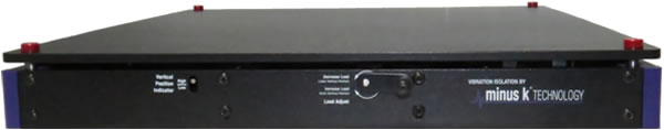
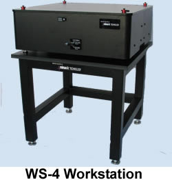
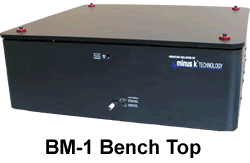
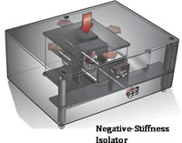
nanoscale research, the Group utilizes Negative-Stiffness vibration isolation,
developed by Minus K Technology, to provide the needed stability for patterning
with atomic force microscopy.
|
|
Organic
semiconductors are non-metallic materials that exhibit semiconductor
properties, whose building blocks are polymers made up of carbon and hydrogen
atoms. Like all semiconductors, the conductivity of semiconducting polymers
changes by orders of magnitude when doped with electron donating or extracting
dopants.
Polymeric semiconductors combine many of the electrical
properties of inorganic semiconductors with the mechanical flexibility and
chemical processability of organic materials.
For instance, solution
processible polymeric semiconductors can be deposited from solution over large
areas or on curved surfaces, greatly reducing production costs compared to
conventional metallic semiconductors. Promising material properties have
motivated a rapid increase in demand for low-cost, high-throughput and
high-resolution fabrication techniques.
Patterning Organic
Semiconductors
Patterning organic semiconductors via traditional
solution-based microfabrication techniques, however, is precluded by undesired
interactions between processing solvents and the organic material. These
materials are generally mutually soluble with other organics, preventing
solution-based deposition of complex patterned structures.
"One of the
really hard problems in solution-processed organic devices is to develop
methods to pattern the organic semiconductor on the nanoscale," said Goktug
Gonel, a researcher with the Moulé Group, at University of California,
Davis. "The reason this problem is difficult, is that fluid dynamics and drying
dominate the deposition process, leaving typical patterns with at least tens of
micrometers in diameter, and uneven thickness."
The Moulé Group
specifically focuses on using structural and dynamic measurement techniques to
quantify the effects of solution processing and patterning on material
morphology and device architecture. The Group is working on a series of
solution-based methods called Dopant Induced Solubility Control that allows the
patterning of organic semiconductors from solution with sub-micron
resolution.
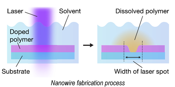
"Dopant Induced Solubility Control presents a relatively new
method for patterning conductive polymers utilizing a change in polymer
solubility," continued Gonel. "By sequentially doping and de-doping films,
polymer solubility can be switched on and off at will. Atomic force microscopy
(AFM) imaging shows that this process is capable of generating both positive
and negative features, with widths and edges sharper than obtainable
previously."
"In addition, by changing the solvent used during
patterning, the same process allows for optical de-doping," added Gonel. "Using
a novel hyperspectral infrared imaging method, photo-induced force microscopy
(PiFM), we find our method allows for optical control of doping level with
similar subdiffraction-limited resolution. Together, our results illustrate how
the ability of dopants to tune not only work function and carrier densities,
but also physical properties such as solubility, along with the wide range of
easily accessible chemistry in these materials, can drastically simplify
solution-based processing of complex structures."
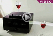
Vibration
Isolation
During semiconductor device manufacturing, wafer testing is
performed, where all individual integrated circuits that are present on the
wafer are tested for functional defects by applying special test patterns. The
wafer testing is performed by a piece of test equipment called a wafer prober.
For electrical testing, a set of microscopic contacts or probes, called a probe
card, are held in place while the wafer, vacuum-mounted on a wafer chuck, is
moved into electrical contact.
The Located on the third floor of a
building on the UC Davis campus, the Moulé Group's nanometer-scale
research is affected by ambient vibrations.
Full article
with Minus K solution... |