|
|
Newsletter March 2021 | Menu of Newsletters

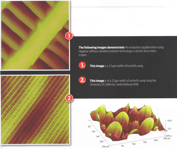
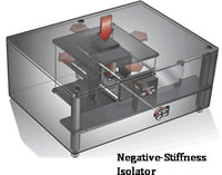
Here is an image of 250 µm width
of butterfly wing using University of California, Santa Barbara AFM with
negative-stiffness
vibration isolation.
(Lagacy 2013 article) With its
development in 1986, and subsequent commercial introduction in 1989, the
atomic force microscope
(AFM) is one of the foremost tools for imaging and measuring
materials and cells on the nanoscale. Revealing sample details at the atomic
level, with resolution on the order of fractions of a nanometer, the AFM is
instrumental for imaging an array of applications, such as defining surface
characterizations, lithography, datastorage, and manipulation of atoms and
nano-sized structures on a variety of surfaces.
The need for more
precise vibration isolation with AFM, though, is becoming critical as
resolutions continue to bridge from micro to nano.
AFM
systems are extremely susceptible to vibrations from the environment. When
measuring a very few angstroms or nanometers of displacement, an absolutely
stable surface must be established for the instrument. Any vibration coupled
into the mechanical structure of the instrument will cause vertical and
horizontal noise and bring about a reduction in the ability to measure with the
highest resolution.
The vertical axis is the most sensitive for AFMs,
but these microscopes are also quite sensitive to vibrations in the X and Y
axes.
The atomic force microscope uses a sharp tip (probe), with a
radius of curvature on the order of nanometers attached to the end of a tiny
cantilever used to scan across a sample surface to image its topography and
material properties. When the tip is brought into proximity of a sample
surface, forces between the tip and the surface lead to a deflection of the
cantilever This deflection is typically recorded using a laser beam that is
reflected from the top surface of the cantilever to a photosensitive detector.
The resultant position change of the cantilever allows characteristics such as
mechanical, electrostatic, magnetic, chemical and other forces to be precisely
measured by the AFM. These characteristics are displayed in a three-dimensional
surface profile of the sample (in the X, Y and Z axes)an advantage that the AFM
can provide compared to other microscopy techniques, such as the scanning
electron microscope (SEM) which delivers a two-dimensional image of a sample
(in the X and Y axes).
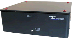
Minus K BM-1
Isolator.
Full article...
|
|
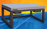
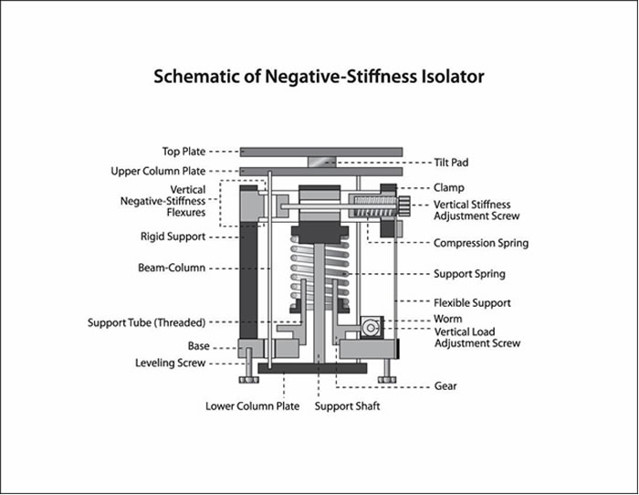
Featured Product: BM-1 Bench Top
Vibration Isolation Platform
- Vertical Load Adjustment
Crank - Simple manual adjustment compensates for changes in vertical load.
- Vertical Load Adjustment
Indicator - Easily determine optimum setting using this simple visual
indicator.
- Vertical Stiffness
Adjustment Screw - Dial in Guaranteed 1/2 Hz or less Vertical natural frequency
using this simple adjustment.
- Isolator Dimensions: 24" W
x 22.5" D x 9" H (610mm W x 572mm D x 216mm H).
- Weight: Approximately 90
lb (41 kg) - Dimensions - an additional 0.675" taller than the above units
Vertical natural frequency of
1/2 Hz or less can be achieved over the entire load range.
Horizontal
natural frequency is load dependent. 1/2 Hz or less can be achieved at or near
the nominal load.
Specifications
(pdf)
Pricing
|

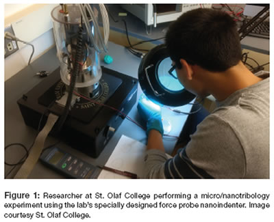
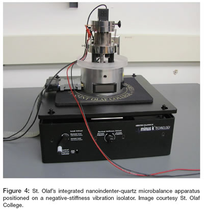
Abstract: Researchers in the Physics
Department of St. Olaf College are using a uniquely designed, integrated
nanoindenter-quartz microbalance apparatus to bridge the gap between the
fundamental science of friction and the engineering of practical
micromechanical systems. This level of micro-research requires extreme
stability for the microbalance instrumentation. Since 2001, the lab has used
negative-stiffness vibration isolation to achieve a high level of isolation in
multiple directions, custom tailoring resonant frequencies to 0.5 Hz vertically
and horizontally.
Introduction: Scientists do not fully
understand what causes friction and wear between two surfaces at the molecular
level. When designing a micromechanical system, the fundamental machine parts
of gears, hinges, pistons, gimbals, and suspended beams that flex are included.
Basic motions that are the essence of mechanics rely on these materials having
durability and low or controllable friction. Mastering these forces that occur
on small-scale surfaces of micromachines is a considerable challenge. When the
mechanical parts are very small, their properties are dominated by minute
surface forces that macroscopic machines are not sensitive enough to detect.
This raises entirely new questions about how to maintain minute components and
to keep them moving and protected from wear or breakage.
Silicon Uniformity:
Engineers have relied on extremely thin
lubricant films to reduce friction and to keep parts moving inside tiny
silicon-constructed microelectromechanical systems (MEMS). But these films have
not been sufficiently effective in micromachines, which rely on relatively
fast-moving parts that are in contact with each other, such as gears, gimbals,
and pistons. Since the early 1980s, with the introduction of the first
micromechanical machines, the vision has been to batch-fabricate these devices
as silicon chips to link with circuitry that can be connected wirelessly.
However, these small silicon machines often disintegrate after just a few hours
of operation. This technology has, for some time, been struggling to make it to
the marketplace. Decades of research in both academia and business has been
undertaken to understand friction and wear well enough at these micro- and
nano-scales to effectively lubricate and provide wear protection.
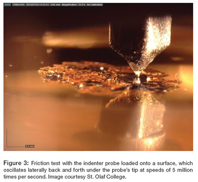
New Research Methodology:
Professor Brian Borovsky,
Associate Professor in the Physics Department at St. Olaf College in
Northfield, MN, has been researching micro/nanotribology for over two decades
[14]. He has pioneered friction research as applied to very tiny
micromechanical machines, having developed state-of-the-art instrumentation and
a process that tests frictional properties of surfaces coated with ultrathin
lubricants. His is one of the few labs that can measure friction of
micromachine surfaces sliding past each other at very high speeds that approach
1m/s.
While equipped with scanning electron (SEM) and atomic force
microscopy (AFM) for analysis of surfaces, the labs focus instrumentation is a
specially designed force probe nanoindenter in conjunction with a quartz
microbalance...
Full article...
|

Commercial Micro Manufacturing -
Dec.2020
The need for nano- precision has became
increasingly important in many fields of research and manufacturing, inducing
microelectromcs fabrication, laser/optical system applications and biological
research. This has meant that so too has the need for vibration Isolation
technology that better facilitates the operation of sensitive Instrumentation
such as
atomic force microscopes, scanning tunneling
microscopes,
laser interferometers and optical
profilers.
Once the mainstay for stabilizing academia's
and Industry's most critical microenginering instrumentation, pneumatic (gas or
air pressurized) vibration Isolation tables are today proving unsatisfactory in
isolating disruptive
low-frequency vibrations. There is a growing trend
for locating sensitive instrumentation in building to locations that are
subject to extremely high levels of vibration and this is a significant
stumbling block for pneumatic vibration isolation tables, meaning alternative
vibration isolation solutions are required.
Vibration
sources
Nano-level instrumentation is sensitive to extremely small
payload vibrations that can be caused by a multitude of factors. Every
structure (building) transmits vibrations from Internal and external sources In
a building, heating and ventilation systems, fans, pumps and elevators are Just
some of the mechanical devices that create vibrations. Outside a building,
adjacent road traffic, nearby construction, aircraft and even wand and other
weather conditions all create vibrations How strongly the instrumentation is
influenced depends on where it is in the building and how far away it is from
the vibration sources.
Isolation for vibration critical applications
Over the
past 25 years, two technologies have gained prominence for their ability to
Isolate vibrations Influencing nano-level Instrumentation, namely active
vibration isolation (also known as electronic-force cancellation) and
negative-stiffness vibration isolation {also known as passive vibration
isolation).
Both active and negative-stiffness vibration isolation are
uniquely equipped for applications where structures smaller than a micrometre
need to be produced or measured. These technologies provide functionality that
is typically not achievable with pneumatic vibration isolation
tables.
Full article: Comparing systems...
|

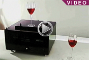
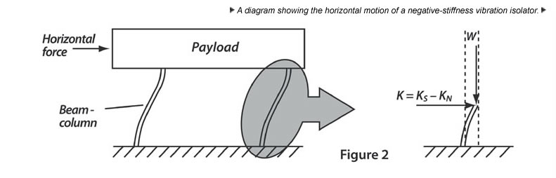
You might have thought, maybe for only a
few moments, that your
audio system was
sounding especially good. With that feeling, you would have rated the sound a
top score of "10". Then those magical moments ended and your system returned to
it's normal - but still good - performance level. Well, folks, the Minus K
CT-2 Isolation
Platform could raise your system score to an "11" and keep it there! Highly
recommended for systems that are already high performance and where you want to
coax the maximum performance from your audio investment....
Dr. David L.
Platus is President and Founder and is the principal inventor of the
technology. He earned a B.S. and a Ph.D. in Engineering from UCLA, and a
diploma from the Oak Ridge School of (Nuclear) Reactor Technology. Prior to
founding Minus K® Technology he worked in the nuclear, aerospace and
defence industries conducting and directing analysis and design projects in
structural-mechanical systems. He became an independent consultant in 1988. Dr.
Platus holds over 20 patents related to shock and vibration
isolation.
Ultra-Thin 2.7" High
CT-2 Product
Attributes:
- Isolation performance is typically 10 to 100 times
better than air systems
- No air or electric power is
required
- Nothing to wear out
- No
maintenance
A complete description of the patented
Negative-stiffness design can be found on the
Technology page of the manufacturers Web site. The Minus K platform is
completely silent and requires no pumps or power. The
CT-2 model platforms
are available for different weight ranges of payload, or supported weight. The
40CT-2 model, while not specifically listed on the Web page, was perfect for
the Clearaudio Ovation
turntable used for
this review. The platform dimensions are 18" W x 20" D x 2.7" H, with a weight
of about 30 pounds. Different models, for different payloads, range in price
from $4,650 to about $5,250. In my system, the platform was installed 20" W x
18" D, which placed the adjustment crank on the 18" left side.
The
horizontal frequency of ~1.5 Hz is achieved at or near the upper limits of the
payload range. The vertical frequency is tunable to 0.5 Hz throughout the
payload range. What this means is that any very low frequency vibrations that
are not blocked or absorbed by the Minus K platform are several orders of
magnitude below what your phono cartridge, or even the best subwoofers, can
process.
Full article...
|

3D Surface Analysis Vibration
Isolation
High-precision, nanometer-level 3D surface
measurement systems can be negatively affected by low-frequency
vibration—distorting imaging and producing inaccurate measurement
readings. |
Manufacturers need to control processes to
produce a consistent, reliable product. Where precision surface engineering is
required, surface measurement may be a key part of maintaining control of the
process, by checking output to see that the process is not outside of
specification.
3D non-contact surface analysis is widely used in the
industry for the measurement of small displacements and surface irregularities.
It delivers the ultimate in high accuracy and repeatable and traceable
measurement. When built into microscopy equipment, employing 3D laser scanning
or structured light, these systems report the surface condition of a product
with more accuracy than any other methodproviding nanometer-level profile
measurements of height, width, angle, radius, volume, and roughness. Such
precision measurement systems allow users to improve product quality and
reliability, and increase manufacturing consistency and production
yields.
Low-Frequency Vibration
When measuring at such high
levels of precision, any instrument can be negatively affected by low-frequency
vibrations generated within a manufacturing facility. These can distort
measurements and impact imaging and measurement data
One company that
has great familiarity with the manufacturing environment and 3D surface
measurements is Keyence Corporation--a leading supplier of sensors, measuring
systems, laser markers, microscopes, and machine vision systems
worldwide.
We have many customers with high-precision 3D measurement
systems operating in high-vibration environments, performing microscopy
evaluation at 30,000 times magnification, looking at nanometer-level surface
features, said Evan Eltinge, Senior Sales Engineer Surface Analysis Team, with
Keyence Corporation of America. At that level of detail, and in that
environment, if measures are taken to reduce vibration it improves the quality
of the data.
Without proper isolation surface measurements occurring at
3,000 to 5,000 times magnification, the vibration could contribute to image
blurring and loss of image quality, continued Eltinge.
Vibration can be
caused by a multitude of factors within a plant; every structure is
transmitting noise. Within the building itself, production machinery, forklift
trucks, the heating and ventilation system, fans, pumps, compressors, and
elevators are just some of the mechanical devices and equipment that create
low-frequency vibration. Depending on how far away the surface measurement
instrumentation is from these vibration sources, and where inside the structure
the instrumentation is locatedwhether on the production floor or in a loftwill
determine how strongly the instrumentation will be influenced.
External
to the building, the equipment can be influenced by vibrations from truck
movement, road traffic, nearby construction, loud noise from aircraft, and even
wind and other weather conditions that can cause movement of the
structure.
Vibration Isolation Options for 3D Surface
Analysis...
Full article...
|

The Moulé Group, at the University
of California/Davis, is interested in the solution processing and patterning of
organic electronic materials for use in devices such as light-emitting diodes,
photovoltaics, transistors, thermoelectric, and chemical sensors. The Group
specifically focuses on using structural and dynamic measurement techniques to
quantify the effects of solution processing and patterning on material
morphology and device architecture.
Tucker Murrey, a doctoral candidate
and published author with the Moulé Group, is actively involved with
researching and designing a scalable optical patterning process for organic
photovoltaic applications.
"Most working organic devices consist of
several layers of material, each having a specific optical and/or electronic
function," said Murrey. "One universal design constraint for complicated device
architectures, like organic field-effect transistors (OFETs), organic
photovoltaics (OPVs) and red-green-blue organic light-emitting diode (OLED)
displays is that they require multiple components patterned laterally and
vertically to operate. Currently, many of these components are comprised of
non-flexible inorganic materials. In order to move towards flexible, all
organic electronic devices, there is a need to develop high precision vertical
and lateral patterning methods that are compatible with solution processing.
mmense efforts in the plastic electronics field have led to
unprecedented progress and continuous improvements in organic photovoltaic
(OPV) performance.
"Given that conventional photolithography technology
techniques are incompatible with polymeric semiconductors, there is a critical
need to develop scalable photopatterning methods capable of laterally
patterning organic semiconducting compounds with sub-micromometer resolution,"
added Murrey. "This patterning process would enable the construction of a
sophisticated OPV architecture designed to increase external quantum
efficiency."
"A scalable process for controlling film topography with
sub-micrometer resolution would represent a substantial development that
enables the advancement of complex organic electronic device architectures,"
continued Murrey.
Photothermal Projection Lithography
The
Moulé Group is working on a series of solution-based methods, one of
which is called Photothermal Projection Lithography for Polymeric
Semiconductors with Sub-diffraction Limited Resolution.
Polymeric
semiconductors combine many of the electrical properties of inorganic
semiconductors with the mechanical flexibility and chemical processability of
organic materials, such as enabling them to be deposited from solution over
large areas, greatly reducing production costs compared to conventional
metallic semiconductors. Developments like this have motivated a rapid increase
in demand for low-cost, high-throughput, and high-resolution fabrication
techniques.
Organic semiconductors are non-metallic materials that
exhibit semiconductor properties, whose building blocks are polymers made up of
carbon and hydrogen atoms. These conductive polymers are, essentially,
electrical insulators, but become conducting when charges are either injected
from electrodes or by photoexcitation, or doping the intentional introduction
of impurities into an intrinsic semiconductor for the purpose of modulating its
electrical, optical, and structural properties.
"Over the past year I
have been upscaling an optical patterning process that our group developed to
make micro-scale electronic devices with these materials," expressed Murrey.
"The overall pattern area was limited to less than one square millimeter. Now
we are trying to upscale the overall patterning area to about one square
centimeter."
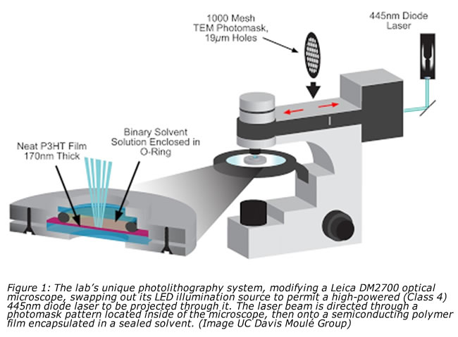
Murrey designed a unique lab-scale photolithography system,
modifying a Leica DM2700 optical microscope, swapping out its LED illumination
source to permit a high-powered (Class 4) 405nm diode laser to be projected
through it. Built into the system is a laser beam expander, collimating lens,
and an optical speckle remover.
 |
Full article...
|
|
|

 |
|
|