![]()
Minus K Educational Giveaway - September 2025
Negative-Stiffness Vibration
Isolation Aids Research for Patterning
Organic Semiconducting Polymers
at Nanoscale Resolutions
The Moulé Group, at the University of California/Davis, has been embarked on a series of solution-based methods, called Dopant Induced Solubility Control, that allow patterning of organic semiconductors from solution with sub-micron resolution. Supporting this nanoscale research, the Group utilizes Negative-Stiffness vibration isolation, developed by Minus K Technology, to provide the needed stability for patterning with atomic force microscopy.
Organic semiconductors are non-metallic materials that exhibit semiconductor properties, whose building blocks are polymers made up of carbon and hydrogen atoms. Like all semiconductors, the conductivity of semiconducting polymers changes by orders of magnitude when doped with electron donating or extracting dopants.
Polymeric semiconductors combine many of the electrical properties of inorganic semiconductors with the mechanical flexibility and chemical processability of organic materials.
For instance, solution processible polymeric semiconductors can be deposited from solution over large areas or on curved surfaces, greatly reducing production costs compared to conventional metallic semiconductors. Promising material properties have motivated a rapid increase in demand for low-cost, high-throughput and high-resolution fabrication techniques.
Patterning Organic Semiconductors
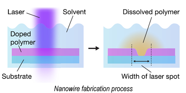
Patterning organic semiconductors via traditional solution-based microfabrication techniques, however, is precluded by undesired interactions between processing solvents and the organic material. These materials are generally mutually soluble with other organics, preventing solution-based deposition of complex patterned structures.
"One of the really hard problems in solution-processed organic devices is to develop methods to pattern the organic semiconductor on the nanoscale," said Goktug Gonel, a researcher with the Moulé Group, at University of California, Davis. "The reason this problem is difficult, is that fluid dynamics and drying dominate the deposition process, leaving typical patterns with at least tens of micrometers in diameter, and uneven thickness."
The Moulé Group specifically focuses on using structural and dynamic measurement techniques to quantify the effects of solution processing and patterning on material morphology and device architecture. The Group is working on a series of solution-based methods called Dopant Induced Solubility Control that allows the patterning of organic semiconductors from solution with
sub-micron resolution.
"Dopant Induced Solubility Control presents a relatively new method for patterning conductive polymers utilizing a change in polymer solubility," continued Gonel. "By sequentially doping and de-doping films, polymer solubility can be switched on and off at will. Atomic force microscopy (AFM) imaging shows that this process is capable of generating both positive and negative features, with widths and edges sharper than obtainable previously."
"In addition, by changing the solvent used during patterning, the same process allows for optical de-doping," added Gonel. "Using a novel hyperspectral infrared imaging method, photo-induced force microscopy (PiFM), we find our method allows for optical control of doping level with similar subdiffraction-limited resolution. Together, our results illustrate how the ability of dopants to tune not only work function and carrier densities, but also physical properties such as solubility, along with the wide range of easily accessible chemistry in these materials, can drastically simplify solution-based processing of complex structures."
Vibration Isolation
The Located on the third floor of a building on the UC Davis campus, the Moulé Group's nanometer-scale research is affected by ambient vibrations.
"We get building vibrations that influence our measurements with the AFM," explained Gonel. "The AFM is in the same room as a glovebox that creates a very noisy environment. We used an optical table for vibration isolation, but still had to be extremely cautious about people walking around and closing doors. Every external vibration would be translated through the equipment and disturb our image quality."
In 2018, the Moulé Group acquired a Negative-Stiffness vibration isolator, which was positioned under the AFM to prevent ambient vibrations from destroying the image quality.
Negative-Stiffness vibration isolation was developed by Minus K Technology, an OEM supplier to leading manufacturers of scanning probe microscopes, micro-hardness testers and other vibration-sensitive instruments and equipment, such as for testing zero-g simulation of spacecraft. The company’s isolators are used by more than 300 universities and government laboratories in 52 countries.
"Minus K's Negative-Stiffness isolator is performing great for us," said Gonel. "We use it actively with the AFM, and have had no issues with vibration-related artifacts. Using Dopant Induced Solubility Control, our Group can characterize patterning features as small as 300 nanometers, as viewed through the AFM."
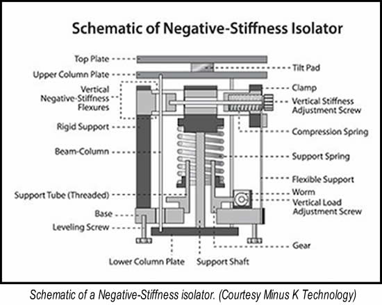
These vibration isolators are compact, and do not require electricity or compressed air which enables sensitive instruments to be located wherever a production facility or laboratory needs to be located. There are no motors, pumps or chambers, and no maintenance because there is nothing to wear out. They operate purely in a passive mechanical mode.
What is very advantageous about Negative-Stiffness isolators is that they achieve a high level of isolation in multiple directions. These isolators have the flexibility of custom tailoring resonant frequencies to 0.5 Hz* vertically and horizontally (with some versions at 1.5 Hz horizontally).
(*Note that for an isolation system with a 0.5 Hz natural frequency, isolation begins at 0.7 Hz and improves with increase in the vibration frequency. The natural frequency is more commonly used to describe the system performance.)
“Vertical-motion isolation is provided by a stiff spring that supports a weight load, combined with a Negative-Stiffness mechanism,” said Erik Runge, Vice President of Engineering at Minus K. “The net vertical stiffness is made very low without affecting the static load-supporting capability of the spring. Beam-columns connected in series with the vertical-motion isolator provide horizontal-motion isolation. A beam-column behaves as a spring combined with a negative-stiffness mechanism. The result is a compact passive isolator capable of very low vertical and horizontal natural frequencies and high internal structural frequencies.”
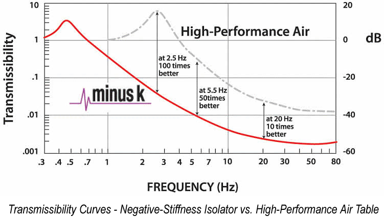
Negative-Stiffness isolators deliver very high performance, as measured by a transmissibility curve. Vibration transmissibility is a measure of the vibrations that are transmitted through the isolator relative to the input vibrations. Negative-Stiffness isolators, when adjusted to 0.5 Hz, achieve approximately 93 percent isolation efficiency at 2 Hz; 99 percent at 5 Hz; and 99.7 percent at 10 Hz.
Nanometer-Scale Imaging
"Our Group has received a NSF-SNM grant to use DISC patterning techniques to generate short-channel transistors made with all polymer materials," explained Gonel. "Negative-Stiffness vibration isolation has been instrumental in providing the needed stability for patterning with atomic force microscopy."
About the Moulé Group, Chemical Engineering Department, University of California, Davis
The Moulé Group is interested in the solution processing and patterning of organic electronic materials for use in devices such as light emitting diodes (LEDs), photovoltaics (PVs), transistors, thermoelectrics and chemical sensors. The Group specifically focuses on using structural and dynamic measurement techniques to quantify the effects of solution processing and patterning on material morphology and device architecture.
|