![]()
Microscopy and Analysis - September 2009
Measuring the Electron Transport Properties of DNA Molecules
Sidney R. Cohen, Claude Nogues and Ron Naaman, Weizmann Institute of Science, Rehovot, Israel
Introduction
Deoxyribonucleic acid (DNA) is a nucleic acid that contains the genetic instructions used in the development and functioning of all known living organisms and some viruses. The main role of DNA molecules is the long-term storage of information. DNA nanotechnology uses the unique molecular-recognition properties of DNA to create self-assembling branched DNA complexes with useful properties. Precisely this self-recognition property has been proposed as a possible approach to molecular electronics: proposals for using DNA to create a self-assembled electronic circuit using this unique self-recognition property, whereby DNA spontaneously organizes into a pre-designed circuit pattern have been forwarded [1]. Such circuitry would require that DNA possesses sufficient electronic conductivity. Furthermore, in natural functioning of DNA, response to and repair of radiation damage likely involves some form of charge transport across significant lengths of the DNA molecules.
Until recently, marked controversy existed regarding the conductive properties of DNA, with experimental results spanning the full range from DNA being a superconductor to a complete insulator. Recent research at the Weizmann Institute of Science has shed new light on the electrical transport properties of DNA, focusing on the mechanism by which short oligomers of DNA mediate current flow along individual strands [2,3,4].
DNA Measurement Challenges
Much of the discrepancy between different laboratories arose from the unique structure of DNA. Even relatively short DNA oligomers, such as those used in this work (26 base pairs) can relax into varied uncontrolled conformations when attached to a solid surface. Another critical issue is formation of a well-characterized electrical contact to the termini of the molecule. The force applied between AFM tip and DNA must be limited so that the delicate molecular structure is not destroyed.
The method developed in our lab addressed these considerations. In order to control the DNA conformation, and prevent unpredictable interactions with the surface, single strands of DNA were chemically bound to a flat gold electrode surface through a gold-thiol covalent bond. This formed the bottom electrical contact. These bound strands were interspersed in a surrounding matrix of a shorter alkanethiol, which prevented them from lying prone on the surface. Separately, a gold nanosphere (GNP) 10 nm in diameter was attached to the complementary strand of this chain. A solution containing this modified strand was then incubated with the modified electrode, so that due to the complementarity, the two strands "hybridized", resulting in a double-stranded (ds) DNA bound to a bottom gold electrode with the GNP forming the upper electric contact (linking of the two single strands, aided by genetic similarity between corresponding DNA sequences).
This preparation method is a fundamental aspect of this research model, and solves the issues of indeterminate configuration of DNA and poorly-defined electrical contact. Furthermore, using this protocol, several controls could be made. Electrical response of the tip could be checked "in-line" with the measurements on the DNA molecules by observing tunneling current through the short thiol molecules.
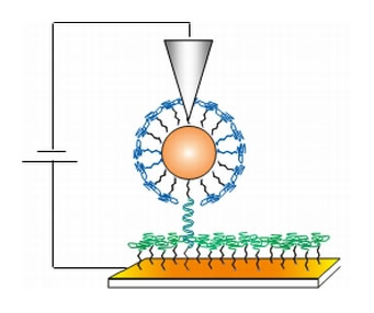 Figure 1: Schematic of the measuring scheme. Single strand DNA was absorbed onto an underlying gold electrode through a thiol linkage. The complementary strand of the DNA was modified by a terminal GNP, and this complex was allowed to hybridize with the bound complementary strand. These complexes were clearly visible in the AFM micrographs due to the protrusions of the GNPs. AFM current measurements were made by placing the AFM tip into contact with the top of the GNP and sweeping the bias between tip and substrate while monitoring current. Reprinted from [2].
The surfaces were imaged and electrically probed using conductive probe atomic force microscopy using an NT-MDT P47 AFM [5] with a MikroMasch NSC36/Ti-Pt tip [7]. A schematic of this technique is shown in Figure 1. In order to avoid damage to the delicate monolayers, imaging was performed in the dynamic (semi-contact) mode. ds-DNA was clearly recognized by the round features representing the gold nanoparticles. Through a custom-designed protocol controlled by the macro-script language of the AFM [6], after locating such a construct in dynamic (also known as semi-contact) mode, the tip was placed directly above it. Then, the conductive AFM tip was lowered vertically into contact with the complex, at a prescribed minimal force (see Figure 2) and current-voltage characteristics were measured. This experimental protocol allowed several controls to be performed in a single scan, comparing measurements on the GNP-DNA complex, the ss-DNA monolayer and on the short alkanethiol matrix. Thus, it was verified that the single strand does not conduct whereas the double strand does. The success of this procedure required stringent environmental conditions: no air currents; good vibration isolation (achieved by using Minus K negative stiffness vibration isolation [8]); and drift compensation. The drift compensation was also controlled through a custom script, using a peak-finding algorithm
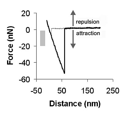 Figure 2: Typical AFM force curve. The gray bar shows the range of forces chosen for contact force during I/V measurements, placed in the attractive force regime so that no compressive force was applied on the DNA strands. Reprinted from [4]
Electron Transport Properties of DNA
DNA is comprised of a sequence of bases. Hybridization of the strands demands that this sequence correspond to a combination of specifically paired "base-pairs". The type and sequence of these base pairs determines the electrical properties: the guanine-cytosine (GC) pair has a lower ionization potential than the thymine-adenine (TA) pair. Thus, the electrical properties may be expected to depend on the relative compositions of these different base pairs. Indeed, the I-V measurements showed just such a difference, as displayed in Figure 3.
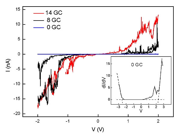
The Figure 3: Typical I/V curves for the 3 different GC-content double strands. Insert: calculated dI/dV curve indicating the calculation of the apparent bandgap. Reprinted from [4].
Four quantities were derived from such curves: (1) The resistance at low voltage bias; (2) The voltage threshold above which current rapidly increases; (3) The effective resistance at high bias; and (4) The maximum current density at 1.5 V bias (presuming all current travels through one ds-DNA chain. In fact, geometrical considerations show that up to three DNA double strands could fit below each GNP so this figure is a maximum, and could be 3 times smaller). The results are displayed in Table I. As is apparent, for increasing GC content, the resistance decreases at both high and low bias, voltage threshold drops, and current density rises. At low bias, the current density increases by 1 order of magnitude for each increment in GC content.
GC content |
Voltage threshold(a) |
Resistivity(b)(Ohms) | V | < 1 V |
Current density at 1.5V c nA/nm2 |
Resistivity (Ohms) | V | > 1 V |
0 |
2.6 +/- 0.09 V |
1414±192 |
0.02 +/- 0.01 |
539±149 |
8 |
1.9 +/- 0.10 V |
605±166 |
0.18 +/- 0.05 |
54±37 |
14 |
0.9 +/- 0.12 V |
29±12 |
1.72 +/- 0.29 |
0.4±0.16 |
Table 1: Summary of current-voltage characteristics. All values reported as mean +/- standard error. (a) Determined from dI/dV curves as indicated in Figure 3. (b) Determined from best fit slope of Current vs. Voltage over indicated range. (c) Calculated presuming all current over a given nanoparticle passes through one ds-DNA.
Conclusions
Two possibilities have been considered for electron flow through a DNA molecule. One is a tunneling process, where the electron effectively shoots through the molecule without localized interactions over the internal structure of the molecule. The other is a hopping process, where the electron actually resides for small periods of time in certain positions along the molecule. The relatively large current densities observed here are not consistent with hopping, and indicate that the electrons interact with a delocalized electronic structure extending over the (backbone) of the complex while passing through the DNA. Therefore, the observed "bandgap" does not represent the total density of states, but rather the density of these delocalized states.
References
1. Braun, E., Eichen, Y., Sivan, U. et al. Nature 1998, 391, 775.
2. Nogues, C., Cohen, S.R., Daube, S.S., Naaman, R. Phys. Chem. Chem. Phys. 2004, 6, 4459.
3. Cohen, H., Nogues, C., Naaman, R., Porath, D. Proc. Natl. Acal. Sci. U.S.A. 2005, 102, 11589.
4. Nogues, C., Cohen S.R., Daube, S., Apter, N., Naaman, R. J. Phys. Chem. B 2006, 110, 8910.
5. NT-MDT, Zelenograd, Russia
6. Power Script, NT-MDT, Zelenograd, Russia.
7. MikroMasch, Tallinn, Estonia
8. Minus K Technology Inc., CA, USA.