
Number 5, December
2009

What's Here for You:
Vibration Isolation News is designed to keep our customers and friends up to date on the latest products and applications designed to facilitate better measurements and improved nanomanufacturing. We are an OEM supplier to leading manufacturers of scanning probe microscopes, micro-hardness testers and other sensitive instruments, and we have users at more than 200 leading universities and private and government laboratories in 35 countries.
INDEX
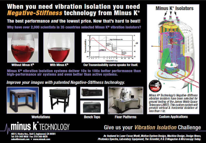
1. Minus K Selected by NASA for JWST
Testing
2. Featured
Application: Brain Waves at Georgetown Univeristy
3. Featured
Product: BM-4 Used by hundreds of customers
4. Another
Enabling Application: Improving AFM Reliability at Arizona
State University
6. Our latest Ad
5. Upcoming Nanotechnology
Meetings and Webinars
7. Your comments and suggestions
We
are proud that our negative stiffness technology is used
by some of the most quality conscious organizations in
the world. The scientists and engineers who have selected
Minus K products have done so because their work requires
the finest vibration isolation.
After considering many alternatives, ITT Space Systems,
LLC, subcontractor to Northrop Grumman Corporation (NYSE:NOC),
selected Minus K to provide vibration isolators for the
ground testing of the new James Webb Space Telescope (JWST)
at the Johnson Space Center (JSC). The JWST will be placed
in a vacuum chamber at the Johnson Space Center and supported
by a set of custom Minus K vibration isolators.
The James Webb Space Telescope is a large aperture infrared
space telescope currently planned to be launched in 2014
from Kourou, French Guiana aboard an Ariane 5 launch vehicle.
JWST is designated to succeed the Hubble Space Telescope
(HST).
A major factor in selecting Minus K is the ability to
not only isolate vibrations vertically, but also horizontally
at less than 1 Hz.
The full story can be found at: http://www.jwst.nasa.gov/
Brain
Waves at Georgetown University
'Dyeing'
to figure out how the brain works
Excerpted
from Medical Design - June 2009
Industry News
 Voltage-sensitive
dye and optical recording techniques are giving neuroscientists
at Georgetown University's Department of Physiology
and Biophysics a new means for figuring out how the
brain works.
Voltage-sensitive
dye and optical recording techniques are giving neuroscientists
at Georgetown University's Department of Physiology
and Biophysics a new means for figuring out how the
brain works.
Professor Jian-Young Wu and his colleagues are conducting
research on waves of neuronal activity. They visualize
wave-like patterns in the brain cortex using a new
method called voltage-sensitive dye imaging. The dye
binds to the membrane of neurons and changes color
when electrical potential changes on the membrane
of active neurons. The neuronal sample is derived
from slices of rat neocortex.
The neocortex is the outer layer of the cerebral hemispheres
in the brain of mammals. Made up of six layers, it
is involved in higher functions such as sensory perception,
generation of motor commands and, in humans, language.
The
neurons of the neocortex are arranged in vertical structures
called neocortical columns. These are patches of the neocortex
with a diameter of about 0.5 mm and a depth of 2 mm. Each
column typically responds to a sensory stimulus representing
a certain body part, or region of sound or vision. In the
human neocortex, there are believed to be about a half-million
of these columns, each of which contains approximately 60,000
neurons.
The neocortex can be viewed as a huge web, consisting of
billions to trillions of neurons and hundreds of trillions
of interconnections. While individual neurons are too simple
to have intelligence, the collective behavior of the billions
of interneuronal interactions occurring each second can
be highly intelligent.
Traditionally, scientists have studied brain activity by
placing a few electrodes in the brain and measuring the
electrical signals of the neurons close to the electrodes.
This method is workable for understanding the function of
the cortex and interactions between individual neurons,
but it is not suitable for studying the emerging properties
of the nervous system.
"It is like viewing a few pixels on a television screen
and trying to figure out the story," explains Wu. "Now,
with optical methods and voltage-sensitive dyes, we can
visualize the activation in a large area of the neocortex
when the brain is processing sensory information, similar
to watching the whole television screen."
"Voltage-sensitive dye is a compound that stains neuronal
membrane and changes its color when the neuron is excited,"
continues Wu. "This allows us to visualize population
neuronal activity dynamically in the cortex. We study how
individual neurons in the neocortex interact to generate
population neuronal activities that underlie sensory and
motor processing functions. Population activities are composed
of the coordinated activity of billions of neurons. Currently,
we study how oscillations and propagating waves can be generated
by small ensembles of neocortical neurons."
Viewing the spatiotemporal patterns of neuronal population
in the cortex is markedly different from recording individual
neurons. Here the cortical activity is viewed as "population
activity," which can be more complex than the linear
addition of an individual neuron's activity. Voltage-sensitive
dye and optical recording techniques give the neuroscientist
new tools for figuring out how brain cortex works.
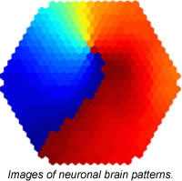
Wu's imaging team has uncovered spiraling wave patterns
resembling little hurricanes in the brain. He believes that
this hurricane-like spiral pattern is an emergent behavior
of the network.
"A metrological hurricane is an emergent behavior of
a large volume of air molecules," says Wu. "If
you were to dissect a hurricane into individual air molecules
you would not find any special process that generates a
hurricane. Similarly, in the nervous system, spiral waves
are an emergent process of the neuronal population and there
might be no special cellular process attributed to spirals."
However, like a hurricane, spiral waves can be a powerful
force. Their power is seen when it comes to organizing the
activity of a neuronal population. Spirals generated in
a small area can send out a powerful storm that invades
large, normal brain areas and starts a seizure attack. This
hypothesis means that epilepsy could be viewed not just
as "mis-wiring" in the brain, but as an abnormal
wave pattern that invades normal tissue.
Similarly, during cardiac fibrillation, spiral waves form
in the heart emitting rotating and scroll waves in two and
three dimensions. As a leading life-threatening situation,
these rotating waves can kill the patient instantly as the
pumping function of the heart is disrupted by the 5 to 10
Hz rotations, which drives chaotic and abnormally rapid
cardiac contractions.
Wu believes that propagating waves are a basic pattern of
cortical neuronal activity, and that these wave patterns
may play an important role in initiating and organizing
brain activity involving millions to billions of neurons.
Studying the spatiotemporal patterns of neuronal population
activity may provide insight into normal brain functions
and pathological disorders. This research has the potential
to help scientists understand abnormal waves that are generated
in the brains of patients with epilepsy.
Since voltage-sensitive dye signals are small - a change
of 0.1 to 1.0 percent of the illumination intensity - Wu's
team uses a high-dynamic-range camera, photodiode array
to detect the voltage- sensitive dye signals of the cortical
activity. The photodiode array can resolve extremely small
changes in light, usually one part of ten thousands. (Human
eyes and ordinary digital cameras register light changes
of one part to a hundred). Detecting such small signals
requires an extreme isolation of vibration. The lab had
to contend with low frequency vibrations from air conditioning
equipment, people walking, and wind blowing against the
building. Vibrations as low as 1 Hz were inhibiting the
integrity of the images and data.
"At first, we used high quality air tables, but they
were not adequate for isolating low frequency vibrations,"
says Wu. "We tried putting a second air table on top
of the first one, but that still did not give us the isolation
we needed. Then we tried an active, electronic system, but
we were still spending much time fighting with floor vibrations.
We were dealing with an unresolved vibration problem for
many years."
The Georgetown lab eventually tested, and settled upon negative-stiffness
mechanism vibration isolation systems from Minus K Technology,
Inglewood, CA, (www.minusk.com) which enabled the lab to
get vibration isolation down to a level of 1 Hz. This effectively
cancelled out any vibration noise difficulties that were
inhibiting image and data readings.
Within the past 10 years, Wu's team has documented a variety
of waveforms (e.g., plane wave and spirals) in brain slices
during artificially induced oscillations. Using neocortical
slices and mathematic models they are studying the initiation
of the waves and the factors that control their propagating
direction and velocity.
The negative-stiffness vibration isolation system are also
used by the lab in the development of optical imaging techniques
such as imaging propagating waves in vivo, within intact
brains. "This is technically difficult," says
Wu. "Other imaging methods (MRI, PET or MEG) provide
inadequate spatiotemporal resolution. Large scale neuronal
activity is a hallmark of a living brain. We hope to visualize
the waves in the cortex in vivo during sensory processes
and in animals while behavioral and cognitive tasks are
performed."
The full
article can be found at: https://minusk.com/content/in-the-news/medical_design_june_2009.html
Featured Product: BM-4 Bench Top Vibration Isolation Platform
The
BM-4 is one of our most popular products. It is the most
cost effective bench top platform capable of 1/2 Hz performance
vertical and horizontal.
Applications have included the full spectrum from Scanning
Probe Microscopes (AFM, STM, NSOM, etc) and Laser/Optical
systems through neurosciences, electronics, and even audio
reproduction.
Because Minus K products can be used under vacuum conditions
and require no power or air for their operation, they
have been used in applications ranging from ground tests
of spacecraft to sensitive experiments where there can
be no stray electromagnetic fields.
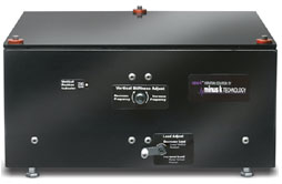
Minus K's BM-4 Bench Top Vibration Isolator
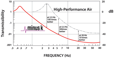
Typical
transmissibility curve with 1/2 Hz natural Frequency
| Load Capacities (approximate): | ||
| Model | Payload Range* | Price** |
| 25BM-4 | 0 - 25 lb : (0 - 11 kg) | $2,750 |
| 50BM-4 | 20 - 55 lb : (9 - 25 kg) | $2,805 |
| 100BM-4 | 50 - 105 lb : (23 - 48 kg) | $2,860 |
| *Contact Minus K for custom payload ranges. |
**For International Orders, A Handling Fee
of 5% is Added. |
|
Performance:
- Vertical natural frequency of 1/2 Hz or less can be achieved over the entire load range.
- Horizontal natural frequency is load dependent. 1/2 Hz or less can be achieved at or near the nominal load.
Negative-stiffness
isolators have resonant frequencies at 0.4 to 0.5 Hz, compared
to 2.3 Hz for pneumatic systems. They transmit less energy
from low-frequency vibrations to the payload than do pneumatic
systems, and maintain better isolation performance through
building frequencies to about 100 Hz.
https://minusk.com/content/products/standard/bm-4.html
Improving
AFM data reliability in nanoelectronics research,
Utilizing negative-stiffness vibration isolation
Excerpted from Electronic Products
& Technology - September 2008
Products on Review
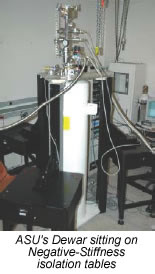
Arizona
State University Nanostructures Research Group, led by ASU
Regents' Professor and nanoelectronics pioneer, David K.
Ferry, Ph.D., M.S.E.E., B.S.E.E., utilizes negative-stiffness
vibration isolation technology to more efficiently eliminate
ultra-low environmental frequencies and improve data set
integrity in nanoelectronics AFM research.
It was
not until Long after 1977 that the name nanoelectronics
came into use, but Dr. David K. Ferry was already actively
engaged in developing some of the world's smallest transistors.
The field, called "Ultra-Small Devices" in the
later part of the 1970's, was in its infancy and Dr. Ferry's
research team was one of only four select groups around
the world aggressively researching the limits of small electronic
devices.
Today, Dr. Ferry heads up the Nanostructures Research Group
at Arizona State University (ASU) in Tempe, a collection
of faculty, staff and students working on research in the
regimes of nanolithography, and the physics of nanostructures
and ultra-small semiconductor devices. The group is part
of the University's College of Engineering, Center for Solid
State Electronics Research, whose alumni makes up a serious
constituency throughout the nanoelectronics universe, in
both industry and academia.
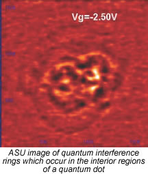
 Their
current interests lie in the area of quantum dots,
quantum wires and ultra-small semiconductor devices
in a variety of materials. The group conducts a
wide spectrum of theoretical studies of quantum
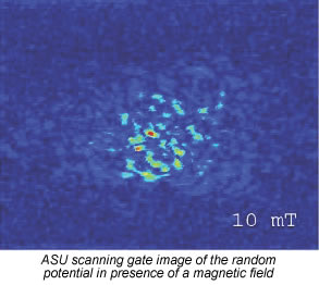
transport in these very small devices. For example,
they are doing a process called scanning gate microscopy
at low temperatures. This involves taking the equivalent
of an atomic force microscope and putting bias on
it and studying the change in conductance of small
semiconductor structures as they move this bias
tip around on a surface.
Their
current interests lie in the area of quantum dots,
quantum wires and ultra-small semiconductor devices
in a variety of materials. The group conducts a
wide spectrum of theoretical studies of quantum
transport in these very small devices. For example,
they are doing a process called scanning gate microscopy
at low temperatures. This involves taking the equivalent
of an atomic force microscope and putting bias on
it and studying the change in conductance of small
semiconductor structures as they move this bias
tip around on a surface.
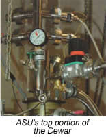
Their
system is mounted in a large cryogenic cooler, an
enclosed container with a helium-3 cooling system,
an isotope of a helium molecule - which is brought
down to 300-milli-Kelvin, or 1,000-times below room
temperature, about one-half degree above absolute
zero. The cooler has a vacuum jacket around it so
the heat can't transmit in, and it protects the cold
from being mitigated by the ambient room temperature.
The Atomic Force Microscope (AFM) tip is on a cantilever. Normally, with the AFM, you just move this cantilever along the surface then note the change in position as it goes over topography on the surface. Dr. Ferry's group is utilizing a process called a piezo-electric sensor. They metalicize the AFM cantilevered tip with a very thin layer of metal so they can apply a voltage to it - then use that voltage to perturb the structure they are looking at. As the tip moves it creates a voltage across the plane, which is measured to determine certain mechanical property values. This is a technique that was developed at Harvard four to five years ago.
This type of experimentation is not uncommon, similar experiments are being done by a large number of universities. But what is not common, is the system that the Nanostructures Research Group is using for vibration isolation: negative-stiffness vibration isolation, developed by Minus K Technology (www. minusk.com) - which provides a significantly greater and more stable attenuation of the critical lower vibration frequencies, and therefore more reliable accrued data sets.
When measuring a very few angstroms or nanometers of displacement, you have got to have an absolutely stable surface upon which to rest your instrument. If you do not, any of that vibration coupled into the mechanical structure of your instrument will cause vertical noise, and fundamentally an inability to measure these kinds of high resolution features.
"Any kind of vibration noise in the system makes that AFM cantilever tip move, and that gives you bad signals and incorrect data," says Dr. Ferry. "We actually went further than most university applications because we integrated a rather large magnet into our system, something that Harvard, for example, is just now putting into their operation. The magnet allows us to look at different types of transport. We can turn the magnet on and look at the magneto-transport of the semiconductors. It is a quite a different mode of transport altogether."
 "The
entire system had to be isolated, not just the cantilever,"
continues Dr. Ferry. "We required an extremely
high level of vibration isolation given our research
parameters. We are deriving modern electronic devices
from our experiments. Future electronic devices
are our interest. What we are doing is looking at
the conductivity of materials and then seeing how
quantum mechanics fits into this. We study basic
physics which has a real application - engineering
- and particularly in the semiconductor industry.
Our research covers:
"The
entire system had to be isolated, not just the cantilever,"
continues Dr. Ferry. "We required an extremely
high level of vibration isolation given our research
parameters. We are deriving modern electronic devices
from our experiments. Future electronic devices
are our interest. What we are doing is looking at
the conductivity of materials and then seeing how
quantum mechanics fits into this. We study basic
physics which has a real application - engineering
- and particularly in the semiconductor industry.
Our research covers:
(1) Electron beam lithography of quantum dots and
quantum devices, with applications such as quantum
ballistic transport at very low temperatures and
high magnetic fields, as well as the quantum-classical
transition, and the role of quantum effects in real
devices at room temperature."
"(2)
Magneto-transport studies used to probe the nature
of electron dynamics in semiconductor quantum dots,
which are quasi-zero-dimensional structures whose
size is comparable to the Fermi wavelength of the
electrons themselves. Magneto-transport studies
may be used to probe these phenomena and to determine
the factors which limit electron phase coherence
within the structures. Current interest in these
devices is motivated by their potential application
in new areas of technology, such as quantum computing
and ultra high frequency signal processing."
"(3) Surface chemical analysis performed with a scanning
Auger microprobe. Under good conditions, a lateral resolution
of about 25 nm is achievable."
 "(4)
Professor Michael Kozicki, in the group, has examined
Chemically Enhanced Vapor Etching (CEVE) patterning
technique. He has used hydrocarbon contamination
layers from laboratory air or vacuum chamber ambients
and successfully demonstrated nanoscale pattern
formation in silicon dioxide. He has also developed
a nitrogen chamber coupled directly to a UHV STM/AFM
facility for CEVE processing of silicon dioxide
resists and their use in semiconductor device fabrication.
Within the nitrogen chamber there is a processing
system for the actual CEVE development."
"(4)
Professor Michael Kozicki, in the group, has examined
Chemically Enhanced Vapor Etching (CEVE) patterning
technique. He has used hydrocarbon contamination
layers from laboratory air or vacuum chamber ambients
and successfully demonstrated nanoscale pattern
formation in silicon dioxide. He has also developed
a nitrogen chamber coupled directly to a UHV STM/AFM
facility for CEVE processing of silicon dioxide
resists and their use in semiconductor device fabrication.
Within the nitrogen chamber there is a processing
system for the actual CEVE development."
"But, the current work with the scanning probe
system is really interesting, and made possible
by the negative-stiffness isolators," says
Dr. Ferry."
The
negative-stiffness isolator is a passive isolation
approach, and has a key advantage in that it is
not powered. It has no electricity going to it.
So, in a site where heat buildup could be an issue,
such as with enclosed cryogenic chambers, negative-stiffness
becomes a highly efficient option.
Negative-stiffness
isolators employ a unique - and completely mechanical -
concept in low-frequency vibration isolation. Vertical-motion
isolation is provided by a stiff spring that supports a
weight load, combined with a negative-stiffness mechanism
(NSM). The net vertical stiffness is made very low without
affecting the static load-supporting capability of the spring.
Beam-columns connected in series with the vertical-motion
isolator provide horizontal-motion isolation. The horizontal
stiffness of the beam-columns is reduced by the 'beam-column'
effect. (A beam-column behaves as a spring combined with
an NSM.) The result is a compact passive isolator capable
of very low vertical and horizontal natural frequencies
and very high internal structural frequencies. The isolators
(adjusted to l/2Hz) achieve 93% isolation efficiency at
2 Hz, 99% at 5 Hz, and 99.7% at l0 Hz.
 Negative-stiffness isolators provide a capability quite
unique to the field of nanotechnology - specifically,
the transmissibility of the negative-stiffness isolator.
That is, the vibration that transmits through the isolator
as measured as a function of floor vibrations - which
is substantially improved over active isolation systems.
Although active isolation systems have fundamentally
no resonance, their transmissibility does not roll off
as fast as negative-stiffness isolators. So, at building
and seismic frequencies the transmissibility of active
isolators can be 10X greater than negative-stiffness
isolators. This causes substantial adverse measurement
and imaging artifacts in the data.
Negative-stiffness isolators provide a capability quite
unique to the field of nanotechnology - specifically,
the transmissibility of the negative-stiffness isolator.
That is, the vibration that transmits through the isolator
as measured as a function of floor vibrations - which
is substantially improved over active isolation systems.
Although active isolation systems have fundamentally
no resonance, their transmissibility does not roll off
as fast as negative-stiffness isolators. So, at building
and seismic frequencies the transmissibility of active
isolators can be 10X greater than negative-stiffness
isolators. This causes substantial adverse measurement
and imaging artifacts in the data.
Compared to other laboratory research instrumentation,
the growth of AFM usage has been quite extensive over
the past 10-years. AFM equipment placement has gone
through a doubling phase pretty much every year during
the last decade. Since its inception in 1988, it has
continuously proven to be a key tool in moving nanotechnology
research forward.
"More than half of the universities in the United States
and worldwide, are engaging in nanotechnology research,"
says Dr. Ferry. "In the electronic area, the nanoelectronic
side of it has been going since the late 1960's. This is
driven by the fact that in the semiconductor industry all
things are getting smaller and smaller. Today, the transistors
have critical dimensions down around 25 nanometers. And
the most critical dimension is the oxide thickness which
is 1 nanometer. When you consider that you have to control
one nanometer vertical thickness over 300-millimeters of
lateral dimension, that is a difference of 10 to the 8th
power. That defines what modern manufacturing technology
produces. The need for effective vibration isolation has
never been greater, and will continue to become more demanding
as the nano-industry progresses."
The
full article can be found at:
https://minusk.com/content/in-the-news/electronic_products&technology_september_2008.html
This ad will be featured in Photonics Online and The Acoustical
Society of America (JASA)
Upcoming Meetings and Webinars:
| Meeting: | Sponsor: | Dates: | Location: |
| SPIE Photonics West | Visit Minus K Booth #5020 at this exhibit | Jan.
26, 2010 - Jan. 28, 2010 |
San Francisco, CA |
| http://spie.org/x2584.xml | |||
| Nanotechnology 10 | WSEAS, IARAS, IASME | Feb.
20, 2010 - Feb. 22, 2010 |
Cambridge, UK |
| http://www.wseas.us/conferences/2010/cambridge/nanotechnology/ | |||
| ICONN 2010 International Conference on Nanoscience and Nanotechnology | Australian Institute of Physics | Feb.
22, 2010 - Feb. 26, 2010 |
Sydney, Australia |
| http://www.ausnano.net/iconn2010/ | |||
| NSTI Nanotech 2010 | Nano
Science and Technology Institute Visit the Minus K Booth at this exhibit |
Jun.
20, 2010 - Jun. 24, 2010 |
Anaheim, CA |
| http://www.techconnectworld.com/Nanotech2010/ | |||
Comments/Suggestions: Applications in New Fields or Features of Interest to You in Our Next Newsletter:
If you want
to share your application with our readers, please send us a description
so that we can publish it in an upcoming newsletter. If you have
comments or suggestions we would be very interested to read them.
Please send any materials to: david.resnik@minusk.com
Tel: 310-348-9656 Fax: 310-348-9638
Contact Us www.MinusK.com
© Minus K Technology Inc., Vibration Isolation Systems. All rights reserved.