![]()
Laser Focus World - April 2023
Combining laser scanning and spectroscopy for enhanced nanolithography patterning
AFM probe for semiconductor patterning, equipped with an aluminum nitrate laser nanowire used as a lithographic tip, allows traditional laser scanning to be performed along with spectroscopy to record a material’s fluorescence signal.
By Jim McMahon
Scanning probe microscopy (SPM) constitutes a family of advanced techniques for surface analysis. The current progress in SPM of polymers, metals, semiconductive, and insulating materials largely stems from the development of atomic force microscopy (AFM). AFM is recognized as a powerful device for obtaining information of material surface structures at the nanoscale. It is used for measuring not only inorganic materials such as metals and semiconductors, but also organic materials and biomaterials.
AFM patterning and imaging techniques are used widely to conduct research into nanoscale device fabrication. In AFM, the sample surface is scanned with a probe consisting of a miniature cantilever and a sharp tip. The tip apex is in continuous contact with the surface when imaging is performed in AFM contact mode, or it is in intermittent contact with the sample in the tapping mode. However, imaging by AFM of high-aspect-ratio nanostructures with sharp edges and straight walls in nanoscale metrology is challenging due to the mechanical properties and conical geometry of most commercially available tips.
Nanowires enhance AFM probe functionality
One-dimensional (1D) semiconductor nanostructures—such as nanowires and nanotubes, commonly defined as linear structures with a diameter less than 100 nm—have emerged as building blocks for the next generation of electronic and optoelectronic nanodevices because of their unique physical and chemical properties.
Gallium nitride (GaN) nanowires are embedded into probes for nanoscale metrology of high-aspect-ratio structures to enhance the resolution of AFM imaging. They also permit combining AFM with other tools such as scanning tunneling microscopy (STM) and near-field scanning optical microscopy (NSOM) to produce a universal multipurpose probe. This combination can be used to enhance lithography and microscopy techniques.
AFM tips for lithography: Laser scanning plus spectroscopy
Pioneering research with GaN nanowire and lasers on AFM probes for use in semiconductor patterning is creating wider possibilities to record not only topography, but also the fluorescence signal of the material.
The Busani Research Group at the University of New Mexico (Albuquerque, NM) is conducting research with 1D nanostructured materials, near-field spectroscopy, nanolasers and nanomembranes, and their integration into multifunctional devices. The group’s multidisciplinary research ranges from photovoltaics and silicon photonics to application of data science techniques in semiconductor research.
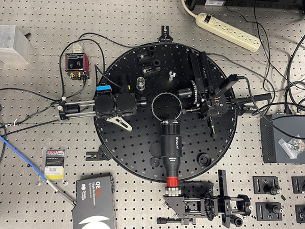
Figure 1. The Busani Research Group’s AFM probe for semiconductor patterning, equipped with an aluminum nitrate laser nanowire used as a lithographic tip, allows traditional laser scanning to be performed along with spectroscopy to record the fluorescence signal of the material.
Tito Busani’s group researches and fabricates lasers and probes used in spectroscopic surface metrology for subnanometer inline lithography. They developed an AFM tip, with a GaN nanowire and laser mounted on the probe, which allows traditional laser scanning to be performed along with spectroscopy recording the fluorescence signal of the material (see Fig. 1).
Busani’s group integrates AFM with a laser tip to probe physical processes and molecular forces. During use of the AFM probe to measure a surface’s topography, the nanowire can be activated via the external laser through an integrated waveguide so that the tip becomes a laser source itself. This means it can be used to radiate the material surface. The light is then collected by the AFM probe itself through the waveguide integrated on the silicon probe, to which the nanowire is attached.
The patterning process, field-emission scanning probe lithography (FE-SPL), a high-resolution method for nanofabrication, is based on the field emission of electrons from ultrasharp tips in close proximity to a sample (distances below 100 nm)—and the emitted electrons expose an ultrathin film.
Busani’s group performs nanofabrication, writing patterns in real time, along with masked lithography alignment. The nanowire being used as a lithographic tip enables self-alignment and dual lithography via either light emission or electron emission.
Vibration isolation
Since Busani’s group deals with nanostructures, ground vibration is important. “We needed an antivibration system for two reasons: for our laser optics, and for our AFM system that we integrate with an external laser source,” Busani says. “The sample that gets exposed to the laser beam on the AFM needs to be optically stable.”
In January 2022, Busani’s group began using negative-stiffness vibration isolators developed by Minus K Technology, an OEM supplier to manufacturers of scanning probe microscopes, micro-hardness testers, and other vibration-sensitive instruments and equipment (see Fig. 2).
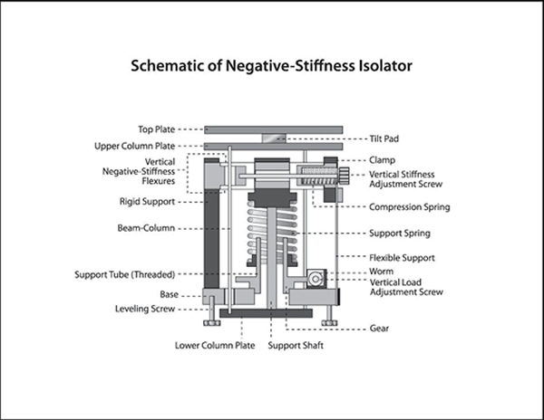
Figure 2. Schematic of the Minus K Technology negative-stiffness isolator.
These vibration isolators are compact and don’t require electricity or compressed air, which enables sensitive instruments to be located wherever they are needed. There are no motors, pumps, or chambers, and no maintenance because there is nothing to wear out. They operate purely in a passive mechanical mode.
Negative-stiffness isolators achieve a high level of isolation in multiple directions, and offer the flexibility of custom tailoring resonant frequencies to 0.5 Hz vertically and horizontally (with some versions at 1.5 Hz horizontally). For an isolation system with a 0.5 Hz natural frequency, isolation begins at 0.7 Hz and improves with increase in the vibration frequency. The natural frequency is more commonly used to describe the system performance.
“Vertical-motion isolation is provided by a stiff spring that supports a weight load, combined with a negative-stiffness mechanism,” says Erik Runge, vice president of engineering for Minus K Technology. “The net vertical stiffness is made very low without affecting the static load-supporting capability of the spring. Beam-columns connected in series with the vertical-motion isolator provide horizontal-motion isolation, and a beam-column behaves as a spring combined with a negative-stiffness mechanism. The result is a compact passive isolator capable of very low vertical and horizontal natural frequencies and high internal structural frequencies.”
Negative-stiffness isolators deliver high performance, as measured by a transmissibility curve. Vibration transmissibility is a measure of the vibrations that are transmitted through the isolator relative to the input vibrations. Negative-stiffness isolators, when adjusted to 0.5 Hz, achieve approximately 93% isolation efficiency at 2 Hz, 99% at 5 Hz, and 99.7% at 10 Hz.
“The negative-stiffness vibration isolation is used for the laser setup to reduce vibration and micromovement,” says Busani. “Stabilizing the sample is critical to reducing noise. The isolator gives better procedural alignment on the tip and allows us to reduce the testing time. Negative-stiffness vibration isolation provides the support needed for the probe’s precision operation.”
Contact: Minus K Technology, Inc., 460 Hindry Avenue, Unit C, Inglewood, CA 90301, 310-348-9656 E-mail: request@minusk.com Web: www.minusk.com