![]()
Laboratory Equipment - June 2007
Laboratory Design & Furnishings
Improving AFM Data Reliability in Nanoelectronics Research
Negative-Stiffness Vibration Isolation Eliminates Ultra-Low Environmental Frequencies and Improves Data Set Integrity
By Jim McMahon
 It was long after 1977 that the name "nanoelectronics" came into use, though Dr. David K. Ferry was already actively engaged in developing some of the world's smallest transistors. The field, which at the time was called "Ultra-Small Devices", was in its infancy and Dr. Ferry's research team was one of only four select groups researching the limits of small electronic devices.
Today, Dr. Ferry heads up the Nanostructures Research Group at Arizona State University (ASU) in Tempe, a collection of faculty, staff and students working on research in the regimes of nanolithography, the physics of nanostructures and ultra-small semiconductor devices. The group is part of the University's College of Engineering, Center for Solid State Electronics Research, whose alumni make up a serious constituency throughout the nanoelectronics universe in both industry and academia.
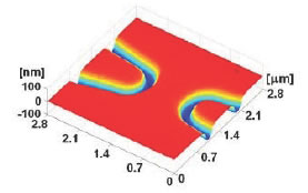
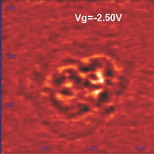
Their current interests lie in the area of quantum dots, quantum wires and ultra-small semiconductor devices in a variety of materials. The group conducts a wide array of theoretical studies of quantum transport in these very small devices. For example, they are involved in a process called scanning gate microscopy at low temperatures. This involves taking the equivalent of an atomic force microscope, putting bias on it, and studying the change in conductance of small semiconductor structures as they move this bias tip around on a surface.
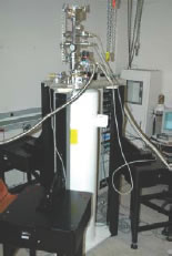
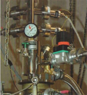
The system is mounted in a large cryogenic cooler, an enclosed container with a helium-3 cooling system, an isotope of a helium molecule-which is brought down to 300 milli-Kelvin, or 1000 times below room temperature, about one-half a degree above absolute zero. The cooler has a vacuum jacket around it so the heat can't transmit in, and it prevents the cold from being mitigated by the ambient room temperature.The AFM tip is on a cantilever. Normally, with the AFM, one moves the cantilever along the surface and then notes the change in position as it goes over topography on the surface. Dr. Ferry's group is utilizing a process called a piezo-electric sensor in which they metalicize the AFM cantilevered tip with a very thin layer of metal so they can apply a voltage to it. They then use that voltage to perturb the structure they are looking at. As the tip moves it creates a voltage across the plane, which is measured to determine certain mechanical property values. This is a technique that was developed four or five years ago at Harvard University.
High Level of Vibration Isolation Required
 When measuring a very few angstroms or nanometers of displacement, an absolutely stable surface upon which to rest your instrument is critical. If not, any of the vibration coupled into the mechanical structure of the instrument will cause vertical noise and fundamentally an inability to measure these kinds of high resolution features.
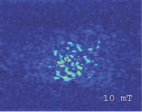
"Any kind of vibration noise in the system makes the AFM cantilever tip move, and that gives you bad signals and incorrect data," says Dr. Ferry. "We actually went further than most university applications because we integrated a rather large magnet into our system, something that Harvard, for example, is just now putting into their operation. The magnet allows us to look at different types of transport. We can turn the magnet on and look at the magneto-transport of the semiconductors. It is a quite a different mode of transport altogether."
"The entire system had to be isolated, not just the cantilever," continues Dr. Ferry. "We required an extremely high level of vibration isolation given our research parameters. We are deriving modern electronic devices from our experiments. Future electronic devices are our interest. What we are doing is looking at the conductivity of materials and then seeing how quantum mechanics fits into this. We study basic physics, which has a real application-engineering-particularly in the semiconductor industry."
Dr. Ferry's Research Covers:
(1) Electron beam lithography of quantum dots and quantum devices, with applications such as quantum ballistic transport at very low temperatures and high magnetic fields, as well as the quantum-classical transition and the role of quantum effects in real devices at room temperature.

(2) Magneto-transport studies used to probe the nature of electron dynamics in semiconductor quantum dots, which are quasi-zero-dimensional structures whose size is comparable to the Fermi wavelength of the electrons themselves. Magneto-transport studies may be used to probe these phenomena and to determine the factors which limit electron phase coherence within the structures. Current interest in these devices is motivated by their potential application in new areas of technology, such as quantum computing and ultra high frequency signal processing.
 (3) Surface chemical analysis performed with a scanning Auger microprobe. Under good conditions, a lateral resolution of about 25 nm is achievable.
(4) Professor Michael Kozicki, in the group, has examined Chemically Enhanced Vapor Etching (CEVE) patterning technique. He has used hydrocarbon contamination layers from laboratory air or vacuum chamber ambients and successfully demonstrated nanoscale pattern formation in silicon dioxide.
He has also developed a nitrogen chamber coupled directly to a UHV STM/AFM facility for CEVE processing of silicon dioxide resists, and their use in semiconductor device fabrication. Within the nitrogen chamber there is a processing system for the actual CEVE development.
 "But, the current work with the scanning probe system is really interesting, and made possible by the negative-stiffness isolators," Dr. Ferry concludes.
The negative-stiffness isolator, a passive isolation approach, has a key advantage in that it is not powered -- it has no electricity going to it. So, in a site where heat buildup could be an issue, such as with enclosed cryogenic chambers, negative-stiffness becomes a highly efficient option.
Negative-stiffness isolators employ a mechanical concept in low-frequency vibration isolation. Vertical-motion isolation is provided by a stiff spring that supports a weight load, combined with a negative-stiffness mechanism (NSM). The net vertical stiffness is made very low without affecting the static load-supporting capability of the spring. Beam-columns connected in series with the vertical-motion isolator provide horizontal-motion isolation. The horizontal stiffness of the beam-columns is reduced by the "beam-column" effect.
(A beam-column behaves as a spring combined with an NSM.) The result is a compact passive isolator capable of very low vertical and horizontal natural frequencies and very high internal structural frequencies. The isolators (adjusted to 1/2 Hz) achieve 93% isolation efficiency at 2 Hz, 99% at 5 Hz, and 99.7% at 10 Hz.
 Negative-stiffness isolators provide a capability quite unique to the field of nanotechnology -- specifically, the transmissibility of the negative-stiffness isolator, that is, the vibration that transmits through the isolator as measured as a function of floor vibrations -- which is substantially improved over active isolation systems. Although active isolation systems fundamentally have no resonance, their transmissibility does not roll off as fast as negative-stiffness isolators. So, at building and seismic frequencies the transmissibility of active isolators can be 10X greater than negative-stiffness isolators. This causes substantial adverse measurement and imaging artifacts in the data.
Compared to other laboratory research instrumentation, the growth of AFM usage has been quite extensive over the past 10 years. AFM equipment placement has gone through a doubling phase pretty much every year during the last decade. Since its inception in 1988, it has continuously proven to be a key tool in moving nanotechnology research forward.
"More than half of the universities in the United States, and worldwide, are engaging in nanotechnology research," says Dr. Ferry. "In the electronic area, the nanoelectronic side of it has been going since the late 1960s. This is driven by the fact that in the semiconductor industry all things are getting smaller and smaller.
Today, the transistors have critical dimensions down around 25 nanometers. And the most critical dimension is the oxide thickness, which is 1 nanometer. When you consider that you have to control one nanometer vertical thickness over 300 millimeters of lateral dimension, that is a difference of 10 to the 8th power. That defines what modern manufacturing technology produces. The need for effective vibration isolation has never been greater, and will continue to become more demanding as the nano-industry progresses."
David K. Ferry, Ph.D., M.S.E.E., B.S.E.E., is a Regents' Professor of Electrical Engineering; recipient of the Arizona State University Graduate Mentor Award, 2001; and recipient of the IEEE Cledo Brunetti Award, 1999 for fundamental contributions to the theory and development of nanostructured devices.
For more information contact Steve Varma at Minus K Technology, Inc at sales@minuk.com or by phone at 310-348-9656.