![]()
Electronic
Products & Technology - May 2014
Nanotechnology
Improving nano-scale imaging of of intergrated micro-Raman/AFM systems using negative-stiffness vibration isolation
By Jim McMahon, instrumentation technology writer
The need for precise vibration isolation with scanning probe microscopy (SPM) and nearfield scanning optical microscopy (NSOM) systems is becoming more critical as resolutions continue to bridge from micro to nano. Whether used in academic labs or commercial facilities, SPM and NSOM systems are extremely susceptible to vibrations from the environment.
When measuring a very few angstroms or nanometers of displacement, an absolutely stable surface must be established for the instrument. Any vibration coupled into the mechanical structure of the instrument will cause vertical and/or horizontal noise and bring about a reduction in the ability to measure high-resolution features. The vertical axis is the most sensitive parameter for SPMs, but these instruments can also be quite sensitive to vibrations in the horizontal axis.
Lab design teams obviously need to plan for these special equipment requirements, as they make decisions regarding building-level isolation techniques and localized techniques. Traditionally, bungee cords and high-performance air tables have been the vibration isolators most used for SPM and NSOM work. The ubiquitous passive-system air tables, adequate until a decade ago, are now being challenged by the more refined imaging requirements. Bench-top air systems provide limited isolation vertically and very little isolation horizontally.
Also at a disadvantage are active isolation systems, known as electronic force cancellation, which use electronics to sense motion and then implement equal amounts of motion electronically to compensate and cancel out the motion. Active systems are somewhat adequate for applications with lasers and optics, since they can start isolating as low as 0.7 Hz. But because they run on electricity, they can be negatively influenced by problems of electronic dysfunction and power modulations, which can interrupt scanning.
Enabling more complex optical measurements
Lately, the introduction of integrated microscopy systems employing multiple scopes is enabling more complex optical measurements, but these systems are also much heavier, and there has been little vibration-isolation technology available for such heavy instrumentation. Air tables, which have been liberally used for optics applications, are not ideal for these nano-scale resolution systems because of their inability to effectively isolate vibrations below 20 Hz. Nor can active systems be used with these newer combination systems because of their inability to handle heavy instrumentation.
 But now, negative-stiffness mechanism (NSM) vibration isolation offers a viable alternative choice for SPM and NSOM systems. This includes applications using atomic force microscopy (AFM) integrated with micro-Raman spectroscopy, where negative-stiffness vibration isolation is particularly well-adapted. In fact, it is the application of negative-stiffness isolation that has enabled AFMs to be truly integrated with micro-Raman. Negative-stiffness isolators can handle the weight of a combined system, as well as isolating the equipment from low-frequency vibrations: a critical set of factors that high-performance air tables and active systems cannot achieve.
The integration of AFM with micro-Raman enables a sizable improvement in data correlation between the two techniques, and expanded Raman measurement and resolution capabilities. Micro-Raman is a spectroscopic NSOM technique used in condensed matter physics and chemistry to study vibrational, rotational and other low-frequency modes in a system.
It relies on scattering of monochromatic light-usually from a laser in the visible, near-infrared or near-ultraviolet range. The laser light interacts with phonons or other excitations in the system, resulting in the energy of the laser photons being shifted up or down. The shift in energy gives information about the phonon modes in the system.
Scanning samples in a micro-Raman system, however, entails problems. As a sample is scanned, even a very flat sample, it is hard to keep the lens-to-sample distance constant. As one goes from pixel to pixel under the lens of a Raman, a mixture of sample and air is sampled in the illuminated voxel (volumetric picture element).
This causes "artifactual" intensity variations in the Raman that are unrelated to the chemical composition of the sample and standard methods of auto-focus are simply not accurate enough for a whole host of problems that are being investigated today. Additionally, the point spread function, which determines the resolution of the Raman image, is significantly broader where there are contributions from the out-of-focus light and this reduces resolution.
The atomic force microscope, a very high resolution type of scanning probe microscope, has demonstrated resolution of fractions of a nanometer, making it one of the foremost tools for imaging, measuring and manipulating matter at the nano scale. The information is gathered by "feeling" the surface with a mechanical probe. Piezoelectric elements that facilitate tiny but accurate and precise movements on electronic command enable the very precise scanning.
The AFM consists of a micro-scale cantilever with a sharp tip (probe) at its end that is used to scan the specimen surface. The cantilever is typically silicon or silicon nitride, with a tip radius of curvature on the order of nanometers. When the tip is brought into proximity with a sample surface, forces between the tip and the sample lead to a deflection of the cantilever. Resultant characteristics- mechanical, electrostatic, magnetic, chemical and other forces-are then measured by the AFM, using, typically, a laser spot reflected from the top surface of the cantilever into an array of photodiodes.
Most systems employing AFM plus Raman execute the two types of scans independently. The recently developed direct integration of Raman spectroscopy with AFM technique, however, has opened the door to significantly improved technique and sample analyses.
Micro-Raman is a micro-technique, but when AFM is added, it becomes a nano-technique. It allows the AFM structural data to be recorded on line and improves the resolution of the Raman information when the nanometric feedback of the system adjusts, with unprecedented precision, the position of each pixel of the sample relative to the lens. The small movements of the AFM stage also provide oversampling: a well-known technique for resolution improvement.
One integrated AFM-Raman system developed by Nanonics Imaging Ltd. (in association with major Raman manufacturers such as Renishaw plc, Horiba JY and others) provides simultaneous and, very importantly, on-line data from both modalities. This advantage addresses critical problems in Raman-including resolution and intensity comparisons in Raman images-while permitting on-line functional characterization such as thermal conductivity, elasticity and adhesion, electrical and other properties. It also provides for new avenues of improved resolution including AFM functioning without optical obstruction, parallel recording with Raman in a wide variety of scanned probe imaging modalities enabling direct and simultaneous image comparison and analysis, and high-resolution Raman mapping.
"Until recently, Raman scattering has remained separate and removed from the proliferation of insights that the scanned probe microscopies can give," says Aaron Lewis, president of Nanonics Imaging, an Israel-based firm that was the first to see the potential of such integration (www.nanonics.co.il). "Without this integration of the systems, investigating a sample with scanned probe microscopy required removing the sample from the micro-Raman spectrometer. This meant that the exact region that was being interrogated by Raman could not be effectively correlated with the chosen SPM imaging technique.
 "Another aspect of optical integration is that SPMs can measure forces, but they cannot measure distribution of light in micro-lasers, silicon-based wave guides, fluorescently stained biological materials, etc. For example, there are many important advances occurring in the application of photonics to silicon structures and plasmonic metals. In the past, these photonic structures were in the micrometer range; now they are nanometric."
The Nanonics platform can be used for structural and photonic characterization, as well as the structural and chemical characterization that is available with AFM and Raman integration.
For these applications, Nanonics Imaging is the innovator of AFM and NSOM systems, including dual tip/sample scanning AFM systems; the industry's first NSOM-AFM cryogenic systems; integrated Raman-AFM systems; and multi-probe AFM and SEM-AFM systems. The company also holds patents to the largest range of unique nano-probes.
These probes form a NanoToolKit for unique characterization platforms with a variety of tasks, such as for nano-photonics, plasmonics, nano-chemical imaging and even nano-chemical deposition based on its singular NanoFountainPen technology. The company is focused on full integration of AFM technology with optics, chemical imaging and other analytical tools
Negative-stiffness vibration isolation
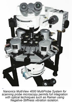
The Nanonics MultiView AFM-NSOM microscope, with its free optical axis on a standard micro-Raman, now makes it possible to truly integrate the separate worlds of Raman and AFM/NSOM nanocharacterization, which has led to a new era in high-resolution Raman spectroscopy.
Facilitating this integration is not only the geometry of the AFM/NSOM platform but also a new generation of AFM glass probes that have very unique characteristics - such as hollow glass probes with cantilevered nano-pippets for material deposition, probes with glass surrounding a single nano-wire in the middle for ultrasensitive electrical measurements. or dual wire glass probes for thermal conductivity and thermocouple measurements. Glass probes are ideal for Raman integration because of their transparency to laser light and no Raman background.
They also expand outward allowing unprecedented correlation of Raman and AFM, also permitting multiple probes to be brought easily together, which is very difficult with a standard AFM.
Enabling AFM and Micro-Raman to Function as an Integrated Platform.
Underlying this pioneering integration AFM with micro-Raman is negative-stiffness vibration isolation, developed by Minus K Technology Inc. What negative-stiffness isolators provide is really quite unique to SPM-Raman and other NSOM systems. In particular, improved transmissibility of a negative-stiffness isolator - that is the vibrations that transmit through the isolator relative to the input floor vibrations. Transmissibility with negative-stiffness is substantially improved over air systems and over active isolation systems.
Negative-stiffness isolators employ a unique, completely mechanical concept for low-frequency vibration isolation. Vertical-motion isolation is provided by a stiff spring that supports a weight load, combined with a negative-stiffness mechanism.
The net vertical stiffness is made very low without affecting the static load-supporting capability of the spring. Beam-columns connected in series with the vertical-motion isolator provide horizontal-motion isolation. The horizontal stiffness of the beam-columns is reduced by the "beam-column" effect (A beam-column behaves as a spring combined with a negative-stiffness mechanism).
The result is a compact passive isolator capable of very low vertical and horizontal natural frequencies and very high internal structural frequencies. The isolators (adjusted to 1/2 Hz) achieve 93% isolation efficiency at 2 Hz; 99% at 5 Hz; and 99.7% at 10 Hz.